Wednesday, January 21, 2009
Nanopore Sensor

Applied voltage draws a DNA strand and surrounding ionic solution through a pore of nanometer dimensions. The various DNA units in the strand block ion flow by differing amounts. In turn, by measuring these differences in ion current, scientists can detect the sequence of DNA units. Atomistic scale simulations performed on the NASA Columbia supercomputer (SGI Altix-3000) allow detailed study of DNA translocation to enhance the abilities of these sequencers. Solid-state nanopores offer a better temporal control of the translocation of DNA, and a more robust template for nano-engineering than biological ion channels. The chemistry of solid-state nanopores can be more easily tuned to increase the signal resolution. These advantages will results in real-time genome sequencing. Potential applications for NASA missions including astronaut health, life detection and decoding of various genomes.
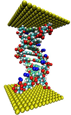
AN ENGINEERED DNA STRAND

An engineered DNA strand between metal atom contacts could function as a molecular electronics device. Such molecules and nanostructures are expected to revolutionize electronics. Understanding the complex quantum physics involved via simulation guides design. For NASA, devices and sensors made from such molecules and nanostructures may be particularly useful when electrical power is limited.
Tuesday, January 20, 2009
nuclear subs
Nuclear subs that course through the blood to shoot cancerous tumours with a laser; self-replicating nanobots that escape from a lab to devour the Earth in a "grey goo" – this is all the stuff of airport novels. The physics at this scale tells us that tiny propellers, for example, simply would not work in the way envisaged.

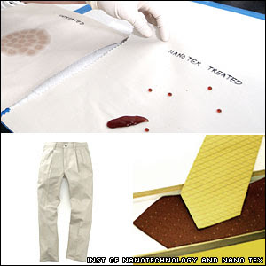
The clothing industry uses nanotech to make stain-repellent fabrics. A chemical process during manufacture forces liquids to bead up when spilled on a garment for easy wiping away. Socks that are made with nano-silver particles give anti-microbial protection, preventing bacteria and fungus that cause itchiness and smells.

Monday, January 12, 2009
An atomic force microscope image of both metallic and semiconducting carbon nanotubes, before the cycloaddition process of removing the metallic tubes

Abstract:
Using a simple chemical process, scientists at Cornell and DuPont have invented a method of preparing carbon nanotubes for suspension in a semiconducting "ink," which can then be printed into such thin, flexible electronics as transistors and photovoltaic materials.
Carbon nanotube 'ink' may lead to thinner, lighter transistors and solar cellsITHACA, NY Posted on January 8th, 2009
The method, which involves treating carbon nanotubes with fluorine-based molecules, is reported in the Jan. 9 issue of the journal Science (Vol. 323 No. 234). The research was jointly led by Graciela B. Blanchet, a research fellow at DuPont, and George Malliaras, Cornell associate professor of materials science and engineering and the Lester B. Knight Director of the Cornell NanoScale Science and Technology Facility. Helen Lu, a research chemist at Dupont, and Mandakini Kanungo, a former Cornell postdoctoral fellow now at Xerox, also worked on the project.Carbon nanotubes are good candidates for transistors in low-cost, printable electronics, but only after large quantities of them have been converted into semiconductors. When carbon nanotubes are grown in the lab, some are semiconducting but others are metallic, and they are difficult to separate from each other.This mix is a major drawback in creating transistors from nanotubes, Malliaras said. The Cornell/DuPont team concentrated on a new, inexpensive way to eliminate the metallic tubes, preparing them for such applications as suspension in semiconducting ink for printing.To do so, the researchers brought fluorine-based molecules into contact with the nanotubes. Through a process called cycloaddition, the fluorine molecules efficiently attacked or converted the metallic nanotubes, leaving the semiconducting tubes alone, and creating a perfect batch of solely semiconducting nanotubes."Our work suggests that careful control of the chemical reaction enables the complete conversion of metallic tubes without the degradation of semiconducting tubes," Blanchet said.The work should lead to exploration of a wide range of devices, such as novel organic photovoltaic structures, Malliaras added.For the past several years, scientists from Cornell and DuPont have worked together on a variety of projects involving flexible electronics. The research is funded by a grant from the U.S. Air Force for developing transistors from carbon nanotubes.
Subscribe to:
Comments (Atom)